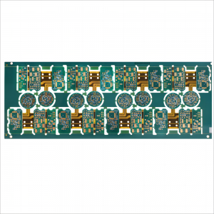
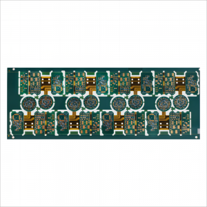
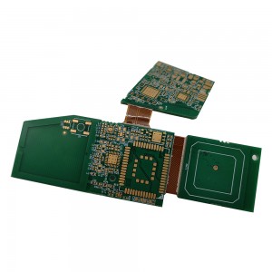
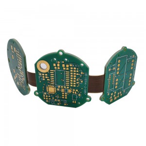
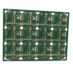
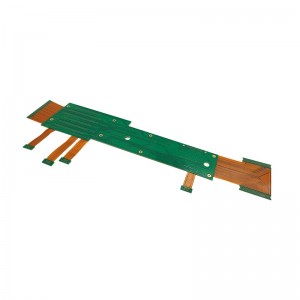
Customized Rigid-Flex PCB circuit board for Bluetooth and Wearable Devices
Basic Info
| Model No. | PCB-A31 |
| Transport package | Vacuum Packing |
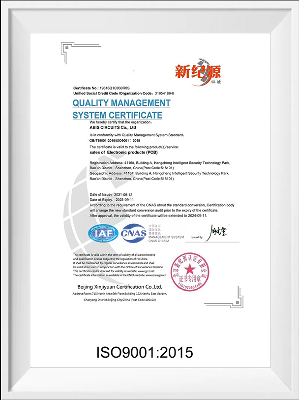
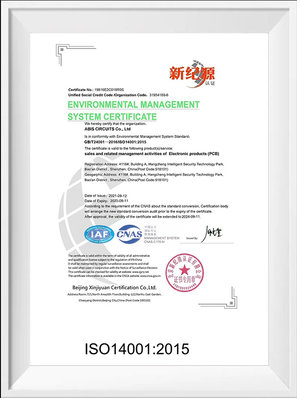
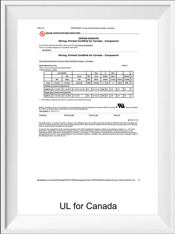
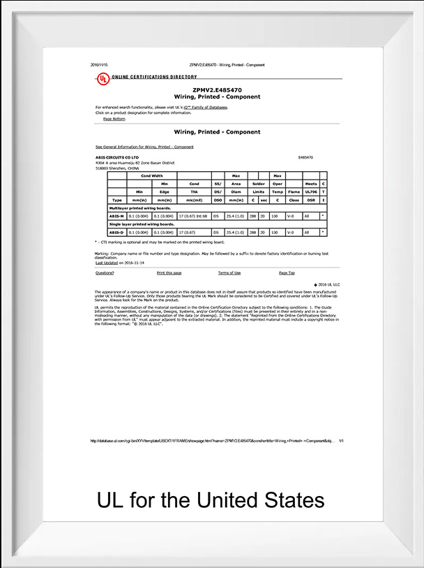
| Certification | UL,ISO9001&ISO14001,RoHS |
| Definitions | IPC Class2 |
| Minimum Space/Line | 0.075mm/3mil |
| Impedance control | 50±10% |
| Production Capacity | 720, 000 M2/Year |
| Origin | Made in China |
Product Description
Rigid-flexible printed circuits boards overview
The literal meaning of "rigid-flex" is combination the advantages of both flexible and rigid boards. It's seen as two-in-one circuit is interconnected through plated thru holes. Rigid flex circuits enable higher component density while fitting into limited and odd shaped spaces.
Rigid-flex printed circuits boards consists of multiple flexible circuit inner layers selectively attached together using an epoxy pre-preg bonding film, similar to a multilayer flexible circuit. Rigid flex circuits have been used in the military and aerospace industries for more than 20 years. In most rigid flex circuit boards.
Technical & Capability
|
Item |
Spec. |
|
Layers |
1~8 |
|
Board Thickness |
0.1mm-8.0mm |
|
Material |
Polymide, PET, PEN, FR4
|
|
Max Panel Size |
600mm×1200mm |
|
Min Hole Size |
0.1mm |
|
Min Line Width/Space |
3mil(0.075mm) |
|
Board Outline Tolerance |
士0.10mm |
|
Insulation Layer Thickness |
0.075mm--5.00mm |
|
Final Thickness |
0.0024''-0.16'' (0.06-2.4.00mm) |
|
Drilling Hole (Mechanical) |
17um--175um |
|
Finish Hole (Mechanical) |
0.10mm--6.30mm |
|
Diameter Tolerance (Mechanical) |
0.05mm |
|
Registration (Mechanical) |
0.075mm |
|
Aspect Ratio |
16:1 |
|
Solder Mask Type |
LPI |
|
SMT Mini. Solder Mask Width |
0.075mm |
|
Mini. Solder Mask Clearance |
0.05mm |
|
Plug Hole Diameter |
0.25mm--0.60mm |
|
Impedance Control Tolerance |
士10% |
|
Surface finish |
ENIG, Chem. Tin/Sn, Flash Gold |
|
Solder mask |
Green/Yellow/Black/White/Red/Blue |
|
Silkscreen |
Red/Yellow/Black/White |
|
Certificate |
UL, ISO 9001, ISO14001, IATF16949 |
|
Special Request |
Blind hole, Gold finger, BGA, Carbon ink, peekable mask, VIP process, Edge plating, Half holes |
|
Material Suppliers |
Shengyi, ITEQ, Taiyo, etc. |
|
Common Package |
Vacuum+Carton |
How ABIS Handling the Flex-Rigid Circuit?
The capability to shape the final assembly of rigid and flexible PCBs to fit a product enclosure is the primary advantage of flexible circuits boards. Here are 2 tips to incorporate in your rigid-flex design project:
Increase trace reliability: The bending that flex circuits endure means that the copper is more likely to delaminate than on a rigid board. The addition of copper to the substrate is less than on an FR4 PCB as well.
Strengthen traces and vias with teardrops: If not controlled, bending the substrate can lead to delamination and product failure. Traces and vias can, however, be strengthened to prevent delamination, also produce better yield in manufacturing by giving more drilling tolerance.
The Advantages about ABIS
- High-end equipment-high speed Pick and Place Machines that can process about 25,000 SMD components per hour
- High efficient supply ability 60K Sqm monthly-Offers low volume and on-demand PCB production, also large-scale production
- Professional engineering team-40 engineers and their own tooling house, strong at OEM. Offers two easy options: Custom and Standard-In-depth knowledge of IPC Class II and III Standards
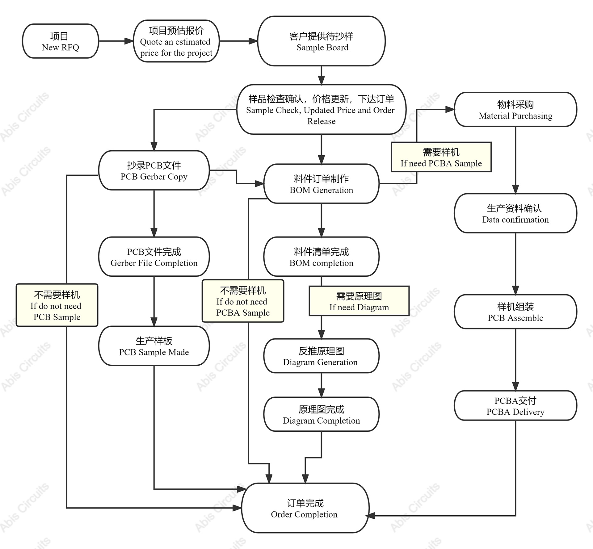
We provide a comprehensive turn-key EMS service to customers who want us to assemble the PCB into PCBA, including prototypes, NPI projects, and small and medium volumes. We are also able to source all components for your PCB assembly project. Our engineers and sourcing team have rich experience in the supply chain and EMS industry, with deep knowledge in SMT assembly allowing us to resolve all the production issues. Our service is cost-effective, flexible, and reliable. We have satisfied customers across many industries including medical, industrial, automotive, and consumer electronics.
Flexible PCB Lead Time
|
Small Batch Volume ≤1 sq meter |
Working Days |
Mass Production |
Working Days |
|
Single-Sided |
3-4 |
Single-Sided |
8-10 |
|
2-4 layers |
4-5 |
2-4 layers |
10-12 |
|
6-8 layers |
10-12 |
6-8 layers |
14-18 |
ABIS Quality Mission
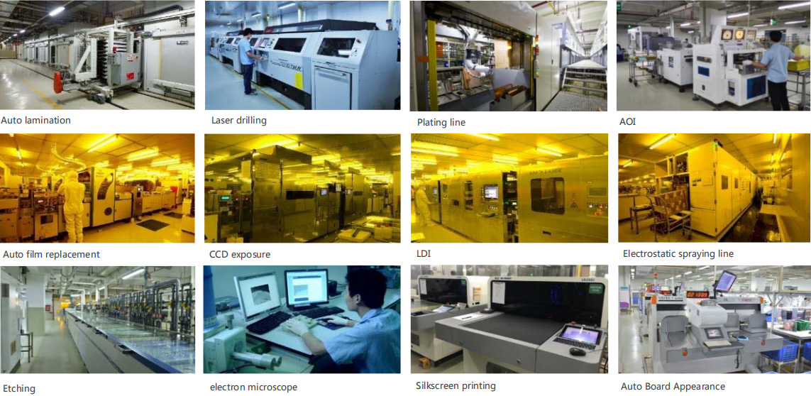
-Advanced equipment LIST
| AOI Testing | Checks for solder pasteChecks for components down to 0201Checks for missing components, offset, incorrect parts, polarity |
| X-Ray Inspection | X-Ray provides high-resolution inspection of:BGAs/Micro BGAs/Chip scale packages /Bare boards |
| In-Circuit Testing | In-Circuit Testing is commonly used in conjunction with AOI minimizing functional defects caused by component problems. |
| Power-up Test |
Advanced Function Test
Flash Device Programming
Functional testing
|
- IOC incoming inspection
- SPI solder paste inspection
- Online AOI inspection
- SMT first article inspection
- External assessment
- X-RAY-welding inspection
- BGA device rework
- QA inspection
- Anti-static warehousing and shipment
-Persue 0% complaint on quality
- All department implements according to ISO and the related dept has to provide 8D report if any board scrapped to defective.
- All the outgoing boards have to be 100% electronic tested, impedance tested and soldering.
- Visual inspected, we make the inspect microsection before shipment.
- Train the mindset of employees and our enterprise culture, make they happy with their work and our company, it's helpful for them to produce good quality products.
- High quality raw material (Shengyi FR4, ITEQ, Taiyo Solder Mask Ink etc.)
- The AOI could inspect the whole set, boards are inspected after each process

Certificate
FAQ
Generally 2-3 days for samples making. The lead time of mass production will depend on the order quantity and the season you place the order.
Our Quality Assuring Procedures as below:
a),Visual Inspection
b),Flying probe, fixture tool
c), Impedance control
d), Solder-ability detection
e), Digital metallograghic microscope
f),AOI (Automated Optical Inspection)
Generally 2-3 days for sample making. The lead time of mass production will depend on the order quantity and the season you place the order.
Our Quality Assuring Procedures as below:
a),Visual Inspection
b),Flying probe, fixture tool
c), Impedance control
d), Solder-ability detection
e), Digital metallograghic microscope
f),AOI (Automated Optical Inspection)
ISO9001, ISO14001,UL USA& USA Canada,IFA16949, SGS, RoHS report.
ABIS's Main Industries: Industrial Control, Telecommunication, Automotive Products and Medical. ABIS's Main Market: 90% International Market(40%-50% for USA, 35% for Europe, 5% for Russia and 5%-10% for East Asia) and 10% Domestic Market.
Please send the details inquiry to us, such as the Item Number, Quantity for each item, Quality request, Logo, Payment Terms, Transport method, Discharge place, etc. We will make an accurate quotation for you as soon as possible.
On time delivery rate is more than 95%
a),24 hours fast turn for double side prototype PCB
b),48hours for 4-8 layers prototype PCB
c),1 hour for quotation
d),2 hours for engineer question/Complaint feedback
e),7-24 hours for technical support/order service/manufacturing operations


